Every chip that powers your phone, laptop, or car is built in a highly controlled environment where even the tiniest particle can ruin an entire batch. Semiconductor manufacturing depends on a resource most people take for granted: water. Not just clean water, but water purified to a level so extreme that it is almost free of measurable impurities. This is known as ultrapure water (UPW) filtration, which forms the foundation of wafer production worldwide.
Fabs cannot run without UPW. They use millions of gallons each day to rinse wafers, mix chemicals, and clean tools. Regular purified water does not meet the strict standards needed. Instead, fabs rely on high-purity water filtration systems that combine membranes, ion exchange, and polishing steps to reach extraordinary quality.
In this blog, we look at how semiconductor water filtration technologies work, why they matter, and how they are expanding into solar and microelectronics industries.
Why does water purity affect electronics yield?
Semiconductor and electronics manufacturing require defect-free surfaces — even a microscopic contaminant can lead to product failure. This is true for chips, solar cells, SSDs, LCDs, and LEDs alike.
What ultrapure water really means
UPW is water treated until it is almost free of measurable impurities like ions, organics, silica, bacteria, and particles. It targets very high resistivity and extremely low total organic carbon.
It is not enough to achieve purity at the central plant. What really matters is the quality of the water at the exact point where it touches the wafer, panel, or circuit. That is why UPW for semiconductor manufacturing and microelectronics includes central treatment, storage, distribution, and final polishing at the point of use.
Many still ask how UPW differs from reverse osmosis water. RO is only a pre-treatment step. UPW goes further with ion exchange or EDI, ultraviolet oxidation, degasification, ultrafiltration, and point-of-use membranes. This broader stack fits the needs of water treatment in the semiconductor industry and electronics manufacturing.
The UPW treatment train from intake to the point of use
Pre treatment
- Intake screening and media filtration to remove suspended solids
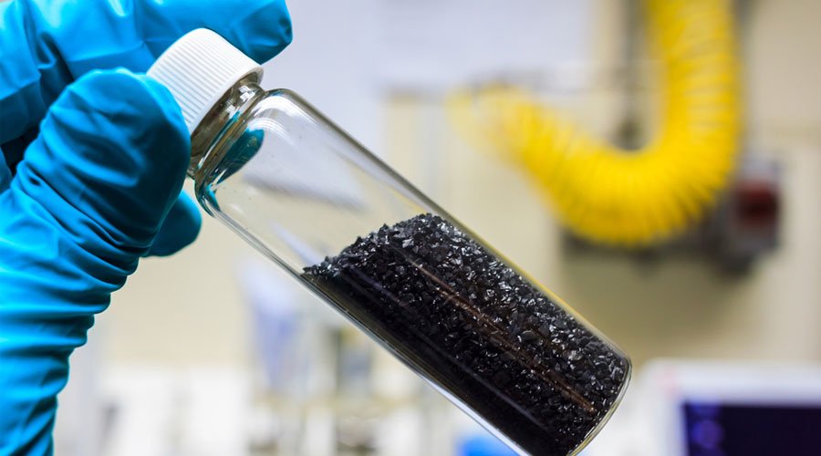
- Activated carbon or advanced adsorbents to reduce organics and chlorine
- Reverse osmosis to remove most dissolved ions and organics
Make-up water and polishing
- Ion exchange or electrodeionisation to reach very high resistivity
- Ultraviolet oxidation to crack trace organics, followed by TOC reduction
- Membrane degasification to remove dissolved oxygen and carbon dioxide
- Ultrafiltration to capture fine colloids and particles ahead of storage
Point of use
- Final membranes tailored to the process step. Here, nanofiltration and microfiltration for UPW protect wafers, panels, and discs at the moment of contact
- Careful piping and valve design to avoid microbial growth or particle shedding
Across these stages, semiconductor water filtration technologies and electronics-grade UPW systems are designed with redundancy, switchover logic, and validated maintenance cycles. The aim is simple: maintain water quality during ramp-up, shift changes, and utility swings without s
Keeping purity stable with monitoring and control
Even the best plant needs tight monitoring. Online sensors track particles, TOC, resistivity, silica, and dissolved gases. Alarms link to interlocks so that off-spec water never reaches production tools. Data is logged for root cause analysis and predictive maintenance.
This operational discipline is part of advanced filtration technologies in semiconductor fabs and electronics plants. Hardware is critical, but so are software controls and operator practices.
Sustainability and water reuse inside fabs
Water supply security is now a strategic issue. Leading fabs and electronics manufacturers reduce intake with internal recycling loops. Rinse streams are cleaned and returned to the UPW plant. Concentrate from RO is diverted to cooling towers or other non-critical uses. Energy efficiency is improved with smarter pumps, low-fouling membranes, and optimised cleaning cycles. These steps protect the supply while reducing the total cost of ownership.
Conclusion
Ultrapure water is the unseen backbone of advanced manufacturing. It safeguards chips, solar cells, storage media, and displays from invisible defects. At Gopani, we design, manufacture, and supply filtration solutions that make this possible.
Our UPW portfolio supports every stage of a plant: pretreatment, make-up water, and polishing before the point of use. With cartridges, capsules, housings, and engineered systems, we help both UPW system builders and end users meet exacting purity standards while improving reliability and sustainability.
Whether your challenge is scaling UPW for semiconductor manufacturing, enabling defect-free microelectronics, or ensuring quality in solar and display technologies, our team brings practical solutions designed for long-term confidence. By focusing on advanced water purification for semiconductors, we ensure fabs and electronics plants have the reliability they need, and UPW system providers have the tools to deliver.